Questions with solutions
Question 1NEET 2026, Q3
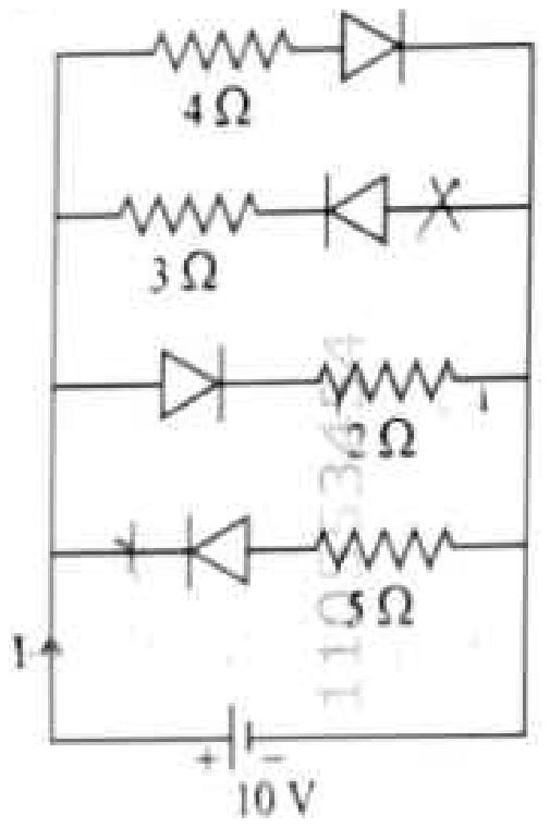
The current I in the circuit shown below is:
(All diodes are ideal and identical)
- 1
- 2
- 3
- 4
Show answer and solution
Correct: option 2,
Current leaves the positive terminal and enters the four branches from the left, so only the diodes pointing from left to right are forward biased: those in the and branches. The diodes in the and branches are reverse biased and carry no current. An ideal forward-biased diode has no voltage drop, so .
Question 2NEET 2026, Q24
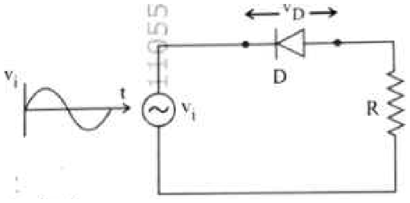
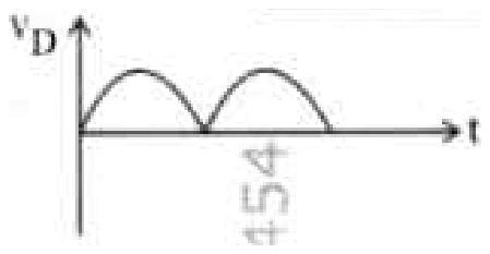
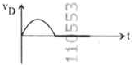
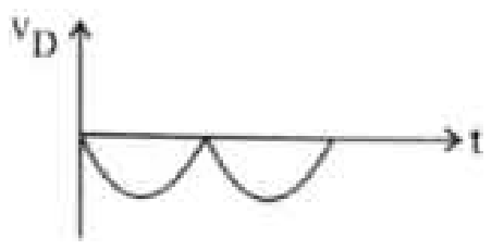
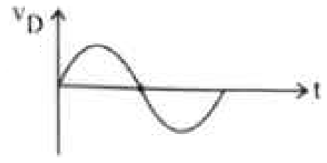
In the circuit shown below, the voltage appearing across the diode D will be of the form:
- 1
- 2
- 3
- 4
Show answer and solution
Correct: option 2
A diode has almost no voltage across it while it conducts, and the whole supply voltage across it while it is reverse biased, because then no current flows and the drop across R is zero. So the diode conducts for one half cycle (zero voltage across it) and blocks for the other half cycle (the full half-wave appears across it). The voltage across D is therefore one half of each cycle followed by zero, as in plot (2).
Question 3NEET 2026, Q44
Two statements are given below:
A. When the forward bias voltage across a p-n junction diode increases above a certain threshold voltage, the diode current increases significantly.
B. This current is called reverse saturation current.
Choose the correct answer from the options given below:
- 1Both Statements A and B are false
- 2Statement A is true, but Statement B is false
- 3Both Statements A and B are true
- 4Statement A is false, but Statement B is true
Show answer and solution
Correct: option 2, Statement A is true, but Statement B is false
Statement A is true: beyond the threshold (cut-in) voltage, about 0.7 V for silicon, the forward current of a diode rises steeply. Statement B is false: the reverse saturation current is the very small, nearly constant current that flows under reverse bias, not the large forward current.
Question 4NEET 2026 Re-exam, Q16
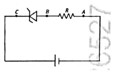
An ideal Zener diode with breakdown voltage of V is reverse biased with a negative input voltage V. The magnitude of voltage difference between points and is:
- 13 V
- 22 V
- 31 V
- 40 V
Show answer and solution
Correct: option 2, 2 V
The 5 V input is larger than the 3 V breakdown voltage, so the Zener diode is in breakdown and holds 3 V across itself (between and ). The rest of the input voltage drops across the series resistor between and : V, option (2).
Question 5NEET 2026 Re-exam, Q42
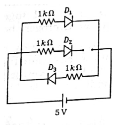
Three identical p-n junction diodes , and are connected across a battery as shown in the figure. If the width of the depletion regions of , and are , and , respectively, then the correct option is:
- 1
- 2
- 3
- 4
Show answer and solution
Correct: option 3,
is forward biased, which narrows its depletion region. The branch of is broken (open), so no voltage acts on it and it keeps its unbiased width. faces the other way and is reverse biased, which widens its depletion region. Hence , option (3).
Question 6NEET 2025, Q8
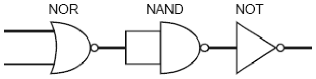
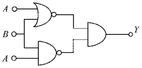
The output (Y) of the given logic implementation is similar to the output of an/a _______ gate.
- 1AND
- 2NAND
- 3OR
- 4NOR
Show answer and solution
Correct: option 4, NOR
The upper gate is a NOR gate giving and the lower gate is a NAND gate giving . The last gate ANDs them: . is 1 only when both inputs are 0, and then is also 1, so . The circuit behaves as a NOR gate, option (4).
Question 7NEET 2025, Q40
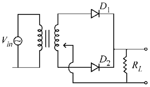
A full wave rectifier circuit with diodes () and () is shown in the figure. If input supply voltage volt, then at msec
- 1 is forward biased, is reverse biased
- 2 is reverse biased, is forward biased
- 3 and both are forward biased
- 4 and both are reverse biased
Show answer and solution
Correct: option 1 or 2
The answer key accepts options 1 and 2.
At ms the phase is , so V: the input is at the peak of its negative half cycle. In a centre-tap full wave rectifier the two ends of the secondary are at opposite potentials, so in any half cycle exactly one diode is forward biased and the other is reverse biased, which rules out options (3) and (4). Which of the two conducts in the negative half cycle depends on the sense of the transformer windings, which the figure does not fix, so the final answer key accepts both option (1) and option (2).
Question 8NEET 2024, Q5
Consider the following statements A and B and identify the correct answer:
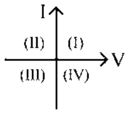
A. For a solar-cell, the I-V characteristics lies in the IV quadrant of the given graph.
B. In a reverse biased pn junction diode, the current measured in (), is due to majority charge carriers.
- 1Both A and B are incorrect.
- 2A is correct but B is incorrect.
- 3A is incorrect but B is correct.
- 4Both A and B are correct.
Show answer and solution
Correct: option 2, A is correct but B is incorrect.
A is correct: a solar cell supplies current to the load instead of drawing it, so with a positive voltage the current is negative and its I-V curve lies in the fourth quadrant. B is incorrect: the small reverse current of a pn junction (a few microamperes) is carried by minority carriers drifting across the junction, not by majority carriers. So the answer is option (2).
Question 9NEET 2024, Q11
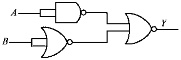
The output () of the given logic gate is similar to the output of an/a:
- 1AND gate
- 2NAND gate
- 3NOR gate
- 4OR gate
Show answer and solution
Correct: option 1, AND gate
The first NAND gate has both inputs joined to , so it gives . The NOR gate has both inputs joined to , so it gives . These two go into a NOR gate: . This is the output of an AND gate, option (1).
Question 10NEET 2024, Q16
A logic circuit provides the output as per the following truth table:
The expression for the output is:
- 1
- 2
- 3
- 4
Show answer and solution
Correct: option 4,
In every row is 1 when is 0 and 0 when is 1, whatever is. So , option (4). Checking option (3): for , it gives 1, which does not match the table.
Question 11NEET 2024 Re-exam, Q17
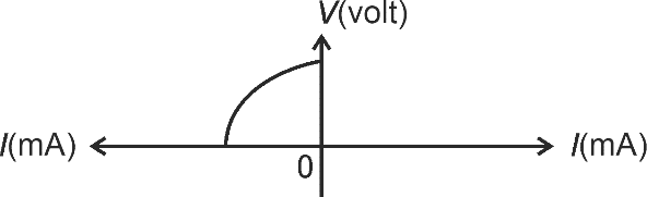
The I-V characteristics shown above are exhibited by a:
- 1Light emitting diode
- 2Zener diode
- 3Photodiode
- 4Solar cell
Show answer and solution
Correct: option 4, Solar cell
The curve does not pass through the origin: it meets the voltage axis at a finite value with no current (the open circuit voltage) and meets the current axis with no voltage (the short circuit current). A device that gives a voltage and a current of its own, with no external bias, is a solar cell. An LED, a Zener diode and a photodiode all need an applied bias.
Question 12NEET 2024 Re-exam, Q29
When the output of an OR gate is applied as input to a NOT gate, then the combination acts as a
- 1NAND gate
- 2NOR gate
- 3AND gate
- 4OR gate
Show answer and solution
Correct: option 2, NOR gate
The OR gate gives and the NOT gate inverts it to , which is the output of a NOR gate.
Question 13NEET 2024 Re-exam, Q48
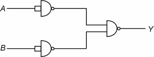
The output for the inputs and of the given logic circuit is:
- 1
- 2
- 3
- 4
Show answer and solution
Correct: option 3,
Each of the first two NAND gates has its two inputs joined, so it works as a NOT gate and gives and . The third NAND gate gives , which by De Morgan's theorem is . The circuit is an OR gate.
Question 14NEET 2023, Q9
A full wave rectifier circuit consists of two p-n junction diodes, a centre-tapped transformer, capacitor and a load resistance. Which of these components remove the ac ripple from the rectified output?
- 1A centre-tapped transformer
- 2p-n junction diodes
- 3Capacitor
- 4Load resistance
Show answer and solution
Correct: option 3, Capacitor
The diodes and the centre-tapped transformer only produce a pulsating one-directional output. The capacitor connected across the load acts as a filter: it charges at the peaks and discharges slowly through the load, smoothing out the ac ripple. So the answer is the capacitor, option (3).
Question 15NEET 2023, Q12
Given below are two statements:
Statement I: Photovoltaic devices can convert optical radiation into electricity.
Statement II: Zener diode is designed to operate under reverse bias in breakdown region.
In the light of the above statements, choose the most appropriate answer from the options given below:
- 1Both Statement I and Statement II are correct.
- 2Both Statement I and Statement II are incorrect.
- 3Statement I is correct but Statement II is incorrect.
- 4Statement I is incorrect but Statement II is correct.
Show answer and solution
Correct: option 1, Both Statement I and Statement II are correct.
Statement I is correct: a photovoltaic device such as a solar cell produces an emf when light falls on its junction. Statement II is correct: a Zener diode is heavily doped and is used in reverse bias in the breakdown region, where its voltage stays nearly constant. Both are correct, option (1).
Question 16NEET 2023, Q42
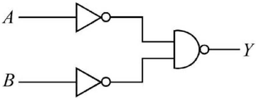
For the following logic circuit, the truth table is:
- 1A B Y
0 0 1
0 1 1
1 0 1
1 1 0
- 2A B Y
0 0 0
0 1 1
1 0 1
1 1 1
- 3A B Y
0 0 1
0 1 0
1 0 1
1 1 0
- 4A B Y
0 0 0
0 1 0
1 0 0
1 1 1
Show answer and solution
Correct: option 2, A B Y
0 0 0
0 1 1
1 0 1
1 1 1
Each input is first inverted by a NOT gate and the two results go into a NAND gate, so by De Morgan's theorem. This is an OR gate: Y is 0 only when both A and B are 0. That is the table in option (2).
Question 17NEET 2023 Manipur, Q2
On the basis of electrical conductivity, which one of the following material has the smallest resistivity?
- 1Glass
- 2Silicon
- 3Germanium
- 4Silver
Show answer and solution
Correct: option 4, Silver
Glass is an insulator (very high resistivity), silicon and germanium are semiconductors (intermediate resistivity) and silver is a metal. Metals have the lowest resistivity, about , so silver has the smallest resistivity.
Question 18NEET 2023 Manipur, Q11
A p-type extrinsic semiconductor is obtained when Germanium is doped with
- 1Arsenic
- 2Boron
- 3Antimony
- 4Phosphorous
Show answer and solution
Correct: option 2, Boron
A p-type semiconductor needs a trivalent (group 13) impurity, which has one valence electron fewer than germanium and so creates a hole. Boron is trivalent. Arsenic, antimony and phosphorus are pentavalent and would give an n-type semiconductor.
Question 19NEET 2023 Manipur, Q16
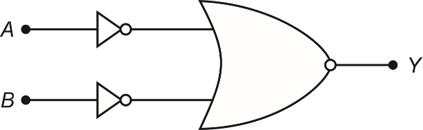
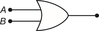
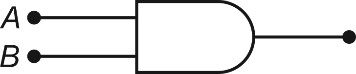
The given circuit is equivalent to
- 1
- 2
- 3
- 4
Show answer and solution
Correct: option 2
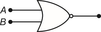
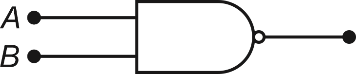
Each input is first inverted by a NOT gate and the two results go into a NOR gate, so . By De Morgan's theorem this equals . That is an AND gate, the symbol in option (2); (1) is OR, (3) is NOR and (4) is NAND.
Question 20NEET 2023 Manipur, Q17
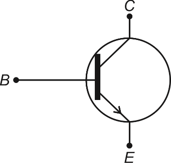
The above figure shows the circuit symbol of a transistor. Select the correct statements given below:
(A) The transistor has two segments of p-type semiconductor separated by a segment of n-type semiconductor.
(B) The emitter is of moderate size and heavily doped.
(C) The central segment is thin and lightly doped.
(D) The emitter base junction is reverse biased in common emitter amplifier circuit.
- 1(A) and (B)
- 2(B) and (C)
- 3(C) and (D)
- 4(A) and (D)
Show answer and solution
Correct: option 2, (B) and (C)
The emitter arrow points away from the base, so this is an n-p-n transistor: two n-type segments separated by a p-type segment. Statement (A) describes a p-n-p transistor, so it is wrong. (B) is correct: the emitter is of moderate size and heavily doped. (C) is correct: the base is thin and lightly doped. (D) is wrong because in an amplifier the emitter-base junction is forward biased. So (B) and (C).
Question 21NEET 2022, Q26
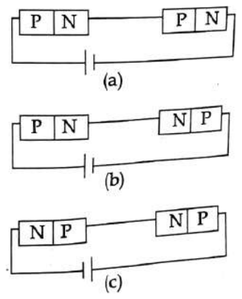
In the given circuits (a), (b) and (c), the potential drop across the two p-n junctions are equal in:
- 1Both circuits (a) and (c)
- 2Circuit (a) only
- 3Circuit (b) only
- 4Circuit (c) only
Show answer and solution
Correct: option 1, Both circuits (a) and (c)
In circuit (a) both junctions point the same way round the loop (P-N then P-N), so both are biased alike and, being in series with the same current, drop equal potentials. The same holds in circuit (c) (N-P then N-P). In circuit (b) the second junction is reversed (P-N then N-P), so one is forward biased and the other reverse biased and the drops are unequal. The answer is both (a) and (c), option (1).
Question 22NEET 2022, Q31
In half wave rectification, if the input frequency is 60 Hz, then the output frequency would be:
- 1120 Hz
- 2zero
- 330 Hz
- 460 Hz
Show answer and solution
Correct: option 4, 60 Hz
A half wave rectifier passes one half of every input cycle, so the output has one pulse per input cycle and its frequency equals the input frequency, 60 Hz, option (4). (A full wave rectifier would give 120 Hz.)
Question 23NEET 2022, Q44
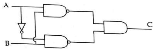
The truth table for the given logic circuit is:
- 1
- 2
- 3
- 4
Show answer and solution
Correct: option 4,
The upper NAND gate gives . A also passes through a NOT gate, so the lower NAND gate gives . The AND gate gives . So C is 1 whenever B is 0, whatever A is: the outputs for AB = 00, 01, 10, 11 are 1, 0, 1, 0, which is the table in option (4).
Question 24NEET 2022 Re-exam, Q18
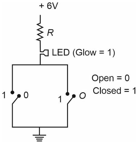
Identify the equivalent logic gate represented by the given circuit
- 1NAND
- 2OR
- 3NOR
- 4AND
Show answer and solution
Correct: option 2, OR
The two switches are in parallel between the LED and the ground. Current flows and the LED glows (output 1) when either switch or both are closed (input 1), and it stays off only when both are open. Output 1 for any input 1 is the OR gate, option (2).
Question 25NEET 2022 Re-exam, Q32
The incorrect statement about the property of a Zener diode is:
- 1p and n regions of zener diode are heavily doped
- 2Zener voltage remains constant at breakdown
- 3It is designed to operate under reverse bias
- 4Depletion region formed is very wide
Show answer and solution
Correct: option 4, Depletion region formed is very wide
A Zener diode has heavily doped p and n regions, which makes its depletion region very thin (less than about m), not wide. It is operated in reverse bias in the breakdown region, where the voltage across it stays constant. So the incorrect statement is option (4).
Question 26NEET 2022 Re-exam, Q49
The collector current in a common base amplifier using n-p-n transistor is 24 mA. If 80% of the electrons released by the emitter is accepted by the collector, then the base current is numerically:
- 13 mA and entering the base
- 26 mA and leaving the base
- 33 mA and leaving the base
- 46 mA and entering the base
Show answer and solution
Correct: option 4, 6 mA and entering the base
, so mA and mA. In an n-p-n transistor the conventional emitter current flows out of the emitter, and it is supplied by currents flowing into the collector and into the base. So the base current is 6 mA entering the base, option (4).
Question 27NEET 2021, Q13
The electron concentration in an n-type semiconductor is the same as hole concentration in a p-type semiconductor. An external field (electric) is applied across each of them. Compare the currents in them.
- 1current in n-type = current in p-type.
- 2current in p-type > current in n-type.
- 3current in n-type > current in p-type.
- 4No current will flow in p-type, current will only flow in n-type.
Show answer and solution
Correct: option 3, current in n-type > current in p-type.
Current is . The carrier concentrations and the field are the same, but electrons have a higher mobility than holes, so the electrons in the n-type drift faster. The current in the n-type is therefore larger.
Question 28NEET 2021, Q23
Consider the following statements (A) and (B) and identify the correct answer.
(A) A zener diode is connected in reverse bias, when used as a voltage regulator.
(B) The potential barrier of p-n junction lies between 0.1 V to 0.3 V.
- 1(A) and (B) both are correct.
- 2(A) and (B) both are incorrect.
- 3(A) is correct and (B) is incorrect.
- 4(A) is incorrect but (B) is correct.
Show answer and solution
Correct: option 3, (A) is correct and (B) is incorrect.
(A) is correct: a zener diode regulates voltage when it works in its reverse breakdown region. (B) is incorrect: the barrier potential is about 0.2 V for germanium and about 0.7 V for silicon, so it does not always lie between 0.1 V and 0.3 V.
Question 29NEET 2021, Q39
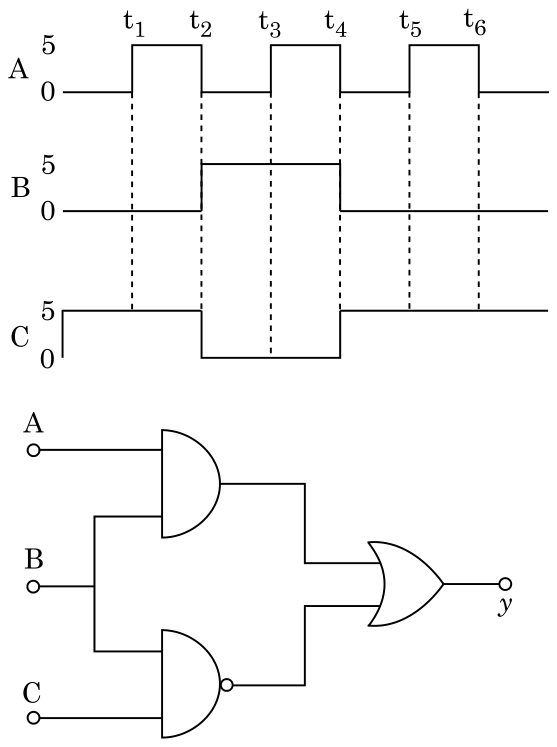
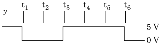
For the given circuit, the input digital signals are applied at the terminals A, B and C. What would be the output at the terminal y?
- 1

- 2
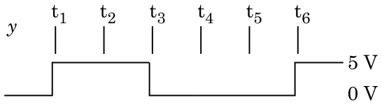
- 3

- 4
Show answer and solution
Correct: option 3
The upper gate is an AND gate giving , the lower gate is a NAND gate giving , and they feed an OR gate: . From the waveforms, B is high only between and , exactly when C is low, so B and C are never high together and the NAND output is always high. The output therefore stays at 5 V all the time, which is option (3).
Question 30NEET 2020, Q138
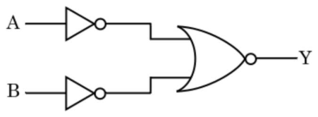
For the logic circuit shown, the truth table is:
- 1
- 2
- 3
- 4
Show answer and solution
Correct: option 1,
Each input passes through a NOT gate, so the NOR gate receives and . Its output is by De Morgan's theorem. The circuit therefore behaves as an AND gate: Y is 1 only when both A and B are 1, which is the first table.
Question 31NEET 2020, Q150
For transistor action, which of the following statements is correct?
- 1Base, emitter and collector regions should have same doping concentrations.
- 2Base, emitter and collector regions should have same size.
- 3Both emitter junction as well as the collector junction are forward biased.
- 4The base region must be very thin and lightly doped.
Show answer and solution
Correct: option 4, The base region must be very thin and lightly doped.
In a transistor the emitter is heavily doped, the base is very thin and lightly doped, and the collector is moderately doped and the largest region, so the three differ in both doping and size. For transistor action the emitter junction is forward biased and the collector junction reverse biased. A thin, lightly doped base lets most of the carriers from the emitter cross to the collector without recombining, so statement (4) is the correct one.
Question 32NEET 2020, Q157
The increase in the width of the depletion region in a p-n junction diode is due to:
- 1forward bias only
- 2reverse bias only
- 3both forward bias and reverse bias
- 4increase in forward current
Show answer and solution
Correct: option 2, reverse bias only
In reverse bias the applied voltage adds to the barrier potential and pulls the majority carriers away from the junction, so more immobile ions are uncovered and the depletion region widens. In forward bias the applied voltage opposes the barrier and the depletion region becomes narrower. So the width increases only under reverse bias.
Question 33NEET 2020 Phase 2, Q92
Which of the following gate is called universal gate?
- 1AND gate
- 2NAND gate
- 3NOT gate
- 4OR gate
Show answer and solution
Correct: option 2, NAND gate
A universal gate is one from which every other gate can be built. NAND gates alone can be combined to make NOT, AND and OR gates, so the NAND gate is a universal gate (NOR is the other one). AND, OR and NOT alone cannot do this.
Question 34NEET 2020 Phase 2, Q103
Out of the following which one is a forward biased diode?
- 1

- 2

- 3

- 4

Show answer and solution
Correct: option 3
In every picture the diode symbol points from left to right, so the left end is the p-side. The diode is forward biased only when the left end is at a higher potential than the right end. That happens only in option (3), where is higher than ; in the others the left end is lower (, , ), so they are reverse biased.
Question 35NEET 2020 Phase 2, Q111
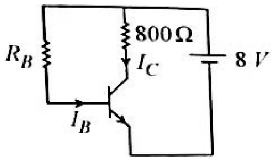
A n-p-n transistor is connected in common emitter configuration (see figure) in which collector voltage drop across load resistance () connected to the collector circuit is 0.8 V. The collector current is,
- 10.1 mA
- 21 mA
- 30.2 mA
- 42 mA
Show answer and solution
Correct: option 2, 1 mA
The collector current flows through the load resistance, so by Ohm's law .
Question 36NEET 2020 Phase 2, Q126
An intrinsic semiconductor is converted into n-type extrinsic semiconductor by doping it with
- 1Aluminium
- 2Silver
- 3Germanium
- 4Phosphorus
Show answer and solution
Correct: option 4, Phosphorus
An n-type semiconductor is made by adding a pentavalent (group 15) impurity. Four of its five valence electrons form bonds with the neighbouring atoms and the fifth is free to conduct. Phosphorus is pentavalent. Aluminium is trivalent and would give a p-type semiconductor, and germanium is itself an intrinsic semiconductor.
Question 37NEET 2019, Q18
For a p-type semiconductor, which of the following statements is true?
- 1Electrons are the majority carriers and trivalent atoms are the dopants.
- 2Holes are the majority carriers and trivalent atoms are the dopants.
- 3Holes are the majority carriers and pentavalent atoms are the dopants.
- 4Electrons are the majority carriers and pentavalent atoms are the dopants.
Show answer and solution
Correct: option 2, Holes are the majority carriers and trivalent atoms are the dopants.
A p-type semiconductor is made by doping silicon or germanium with a trivalent element such as boron, aluminium or indium. Each dopant atom is one electron short of completing four bonds and so creates a hole. Holes are therefore the majority carriers.
Question 38NEET 2019, Q39
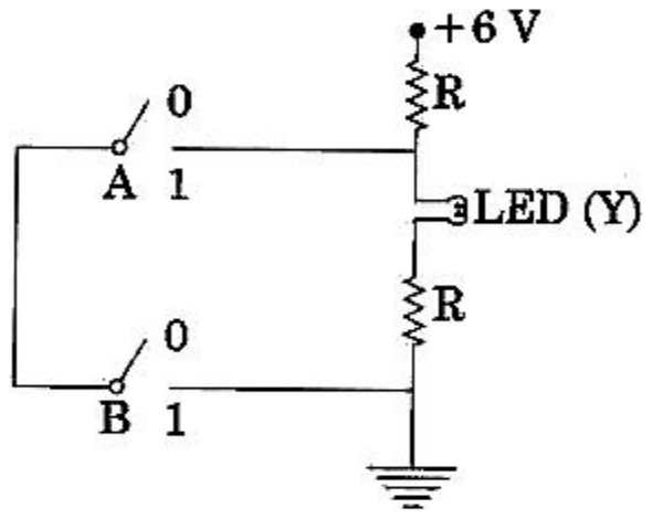
The correct Boolean operation represented by the circuit diagram drawn is:
- 1AND
- 2OR
- 3NAND
- 4NOR
Show answer and solution
Correct: option 3, NAND
The two switches are in series with each other and together they are in parallel with the LED and its lower resistor. Only when both A and B are closed (1, 1) is the LED short-circuited and off; for every other combination the LED glows. Output 0 only for inputs 1, 1 is the NAND operation.
Question 39NEET 2019 Odisha, Q19
An LED is constructed from a p-n junction diode using GaAsP. The energy gap is 1.9 eV. The wavelength of the light emitted will be equal to
- 1
- 2 m
- 3 m
- 4654 nm
Show answer and solution
Correct: option 4, 654 nm
The photon energy equals the energy gap, so nm, which is red light.
Question 40NEET 2019 Odisha, Q20
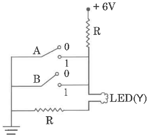
The circuit diagram shown here corresponds to the logic gate,
- 1OR
- 2NAND
- 3NOR
- 4AND
Show answer and solution
Correct: option 3, NOR
With both switches at 0 (open) the current from +6 V flows through the LED and it glows, so Y = 1. If either A or B is at 1 (closed), that switch joins the point above the LED directly to ground, the LED is bypassed and Y = 0. The output is 1 only when both inputs are 0, which is the NOR gate.
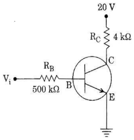
Question 41NEET 2018, Q15
In the circuit shown in the figure, the input voltage is 20 V, and . The values of , and are given by
- 1
- 2
- 3
- 4
Show answer and solution
Correct: option 4,
With , . With , . Then .
Question 42NEET 2018, Q16
In a p-n junction diode, change in temperature due to heating
- 1does not affect resistance of p-n junction
- 2affects only forward resistance
- 3affects only reverse resistance
- 4affects the overall V – I characteristics of p-n junction
Show answer and solution
Correct: option 4, affects the overall V – I characteristics of p-n junction
Heating breaks more covalent bonds and so raises the number of charge carriers. This changes both the forward current and the reverse saturation current, so both forward and reverse resistance change. The whole V – I characteristic of the junction is affected.
Question 43NEET 2018, Q17
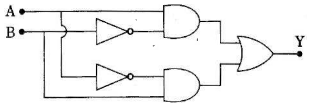
In the combination of the following gates the output Y can be written in terms of inputs A and B as
- 1
- 2
- 3
- 4
Show answer and solution
Correct: option 2,
The upper AND gate receives A and inverted B, giving . The lower AND gate receives inverted A and B, giving . The OR gate adds them: .
Question 44NEET 2017, Q21
In a common emitter transistor amplifier the audio signal voltage across the collector is 3 V. The resistance of collector is 3 k. If current gain is 100 and the base resistance is 2 k, the voltage and power gain of the amplifier is:
- 1200 and 1000
- 215 and 200
- 3150 and 15000
- 420 and 2000
Show answer and solution
Correct: option 3, 150 and 15000
Voltage gain is . Power gain is current gain times voltage gain: .
Question 45NEET 2017, Q22
Which one of the following represents forward bias diode?
- 1

- 2

- 3

- 4

Show answer and solution
Correct: option 1
A diode is forward biased when its p-side (the flat base of the triangle in the symbol) is at a higher potential than its n-side (the bar). In every picture the p-side is on the left. Only in option (1) is the left end higher: 0 V against V. In the others the left end is lower ( V against V, V against V, 3 V against 5 V), so those diodes are reverse biased.
Question 46NEET 2017, Q24
The given electrical network is equivalent to:

- 1AND gate
- 2OR gate
- 3NOR gate
- 4NOT gate
Show answer and solution
Correct: option 3, NOR gate
The first gate is a NOR gate, giving . The second NOR gate has its two inputs joined, so it works as a NOT gate and gives . The last gate is a NOT gate, giving again. So the whole network is a NOR gate.
Question 47NEET 2016 Phase 1, Q13
Consider the junction diode as ideal. The value of current flowing through AB is:

- 10 A
- 2 A
- 3 A
- 4 A
Show answer and solution
Correct: option 2, A
A is at the higher potential, so the diode is forward biased and, being ideal, has no voltage drop. The current is A.
Question 48NEET 2016 Phase 1, Q17
A npn transistor is connected in common emitter configuration in a given amplifier. A load resistance of is connected in the collector circuit and the voltage drop across it is 0.8 V. If the current amplification factor is 0.96 and the input resistance of the circuit is , the voltage gain and the power gain of the amplifier will respectively be:
- 14, 3.84
- 23.69, 3.84
- 34, 4
- 44, 3.69
Show answer and solution
Correct: option 1, 4, 3.84
Taking the given current amplification factor 0.96 as the current gain, voltage gain current gain . Power gain current gain voltage gain .
Question 49NEET 2016 Phase 1, Q34
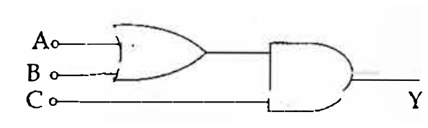
To get output 1 for the following circuit, the correct choice for the input is:
- 1A = 0, B = 1, C = 0
- 2A = 1, B = 0, C = 0
- 3A = 1, B = 1, C = 0
- 4A = 1, B = 0, C = 1
Show answer and solution
Correct: option 4, A = 1, B = 0, C = 1
A and B feed an OR gate whose output goes with C into an AND gate, so . For , C must be 1 and at least one of A and B must be 1. Only A = 1, B = 0, C = 1 satisfies this.
Question 50NEET 2016 Phase 2, Q43
For CE transistor amplifier, the audio signal voltage across the collector resistance of 2 k is 4 V. If the current amplification factor of the transistor is 100 and the base resistance is 1 k, then the input signal voltage is
- 110 mV
- 220 mV
- 330 mV
- 415 mV
Show answer and solution
Correct: option 2, 20 mV
Collector current mA. Base current A. Input signal voltage mV, option (2).
Question 51NEET 2016 Phase 2, Q44
The given circuit has two ideal diodes connected as shown in the figure below. The current flowing through the resistance will be
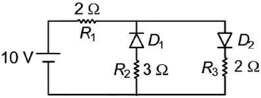
- 12.5 A
- 210.0 A
- 31.43 A
- 43.13 A
Show answer and solution
Correct: option 1, 2.5 A
Diode is reverse biased (its cathode faces the positive side of the battery), so no current flows through the branch with . Diode is forward biased and, being ideal, acts as a plain wire. The current therefore flows through and in series: A, option (1).
Question 52NEET 2016 Phase 2, Q45
What is the output in the following circuit, when all the three inputs , , are first 0 and then 1?

- 10, 1
- 20, 0
- 31, 0
- 41, 1
Show answer and solution
Correct: option 3, 1, 0
Gate P is an AND gate with inputs and ; gate Q is a NAND gate with inputs P's output and . With all inputs 0: P gives 0, and NAND of (0, 0) is 1. With all inputs 1: P gives 1, and NAND of (1, 1) is 0. So is 1, then 0, option (3).
Question 53AIPMT 2015, Q152
Which logic gate is represented by the following combination of logic gates?
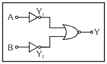
- 1NAND
- 2AND
- 3NOR
- 4OR
Show answer and solution
Correct: option 2, AND
The two input gates are NOT gates, so and . These feed a NOR gate, so . By De Morgan's theorem this equals , which is the AND operation: the output is 1 only when both inputs are 1. Option (2).
Question 54AIPMT 2015, Q172
If in a p-n junction, a square input signal of 10 V is applied as shown,
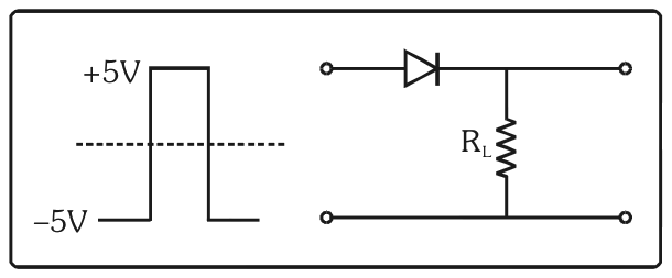
then the output across will be:
- 1
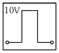
- 2
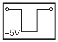
- 3
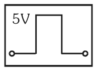
- 4
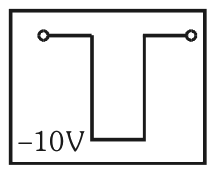
Show answer and solution
Correct: option 3
The diode in series with acts as a half-wave rectifier. The input swings between +5 V and -5 V (10 V peak to peak). During the +5 V part the diode is forward biased and, taken as ideal, passes the full +5 V to ; during the -5 V part it is reverse biased and the output is zero. The output is therefore a positive pulse of height 5 V, which is option (3).
Question 55AIPMT 2015 Re-test, Q150
In the given figure, a diode D is connected to an external resistance and an e.m.f. of 3.5 V. If the barrier potential developed across the diode is 0.5 V, the current in the circuit will be:
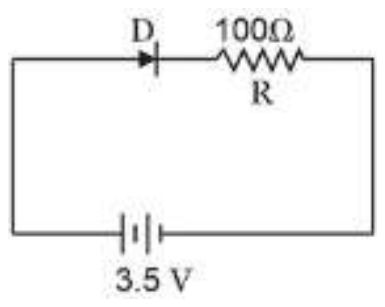
- 135 mA
- 230 mA
- 340 mA
- 420 mA
Show answer and solution
Correct: option 2, 30 mA
The diode is forward biased and drops 0.5 V, leaving across the resistance. .
Question 56AIPMT 2015 Re-test, Q173
The input signal given to a CE amplifier having a voltage gain of 150 is . The corresponding output signal will be:
- 1
- 2
- 3
- 4
Show answer and solution
Correct: option 1,
The amplitude is multiplied by the gain: . A common-emitter amplifier also inverts the signal, a phase shift of , so the phase becomes . Output .
Question 57AIPMT 2014, Q114
The barrier potential of a p-n junction depends on:
(a) type of semi conductor material
(b) amount of doping
(c) temperature
Which one of the following is correct?
- 1(a), (b) and (c)
- 2(a) and (b) only
- 3(b) only
- 4(b) and (c) only
Show answer and solution
Correct: option 1, (a), (b) and (c)
The barrier potential depends on the material (about 0.7 V for silicon, 0.3 V for germanium), on the doping level (heavier doping gives a larger barrier) and on temperature (it falls as temperature rises). All three matter, so option (1) is correct.
Question 58AIPMT 2014, Q116
The given graph represents V - I characteristic for a semiconductor device.
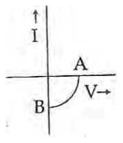
Which of the following statement is correct?
- 1It is for a LED and points A and B represents open circuit voltage and short circuit current respectively.
- 2It is V - I characteristic for solar cell where point A represents open circuit voltage and point B short circuit current.
- 3It is for a solar cell and points A and B represent open circuit voltage and current, respectively.
- 4It is for a photodiode and points A and B represent open circuit voltage and current, respectively.
Show answer and solution
Correct: option 2, It is V - I characteristic for solar cell where point A represents open circuit voltage and point B short circuit current.
The curve lies in the fourth quadrant (positive voltage, negative current), which is the characteristic of a solar cell delivering power. Point A is on the voltage axis where the current is zero, so it is the open circuit voltage; point B is on the current axis where the voltage is zero, so it is the short circuit current. That is option (2).
Question 59NEET 2013, Q151
In a n-type semiconductor, which of the following statement is true:
- 1Electron are minority carriers and pentavalent atoms are dopants.
- 2Holes are minority carriers and pentavalent atoms are dopants.
- 3Holes are majority carriers and trivalent atoms are dopants.
- 4Electrons are majority carriers and trivalent atoms are dopants.
Show answer and solution
Correct: option 2, Holes are minority carriers and pentavalent atoms are dopants.
An n-type semiconductor is made by doping with pentavalent atoms such as phosphorus or arsenic, each of which donates one extra electron. Electrons are therefore the majority carriers and holes the minority carriers.
Question 60NEET 2013, Q152
In a common emitter (CE) amplifier having a voltage gain G, the transistor used has transconductance 0.03 mho and current gain 25. If the above transistor is replaced with another one with transconductance 0.02 mho and current gain 20, the voltage gain will be:
- 11.5 G
- 2 G
- 3 G
- 4 G
Show answer and solution
Correct: option 4, G
Voltage gain of a CE amplifier is , the transconductance times the load resistance. The load is unchanged, so the gain scales with : new gain .
Question 61NEET 2013, Q172
The output (X) of the logic circuit shown in figure will be:

- 1
- 2
- 3
- 4
Show answer and solution
Correct: option 2,
The first gate is a NAND gate, giving . The second NAND gate has its two inputs joined, so it works as a NOT gate and inverts this. The output is , an AND operation.
Question 62NEET 2013 Karnataka, Q139
The output from a NAND gate is divided into two in parallel and fed to another NAND gate. The resulting gate is a:
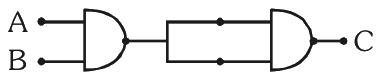
- 1AND gate
- 2NOR gate
- 3OR gate
- 4NOT gate
Show answer and solution
Correct: option 1, AND gate
The first gate gives . A NAND gate with both inputs joined acts as a NOT gate, so the second gate inverts this: . The combination is an AND gate.
Question 63NEET 2013 Karnataka, Q164
One way in which the operation of a n-p transistor differs from that a p-n-p:
- 1The emitter junction injects minority carriers into the base region of the p-n-p
- 2The emitter injects holes into the base of the p-n-p and electrons into the base regions of n-p-n
- 3The emitter injects holes into the base of n-p-n
- 4The emitter junction is reversed biased in n-p-n
Show answer and solution
Correct: option 2, The emitter injects holes into the base of the p-n-p and electrons into the base regions of n-p-n
The emitter sends its own majority carriers into the base. In a p-n-p transistor the emitter is p-type and injects holes; in an n-p-n transistor the emitter is n-type and injects electrons. The emitter junction is forward biased in both.
Question 64NEET 2013 Karnataka, Q179
In an unbiased p-n junction, holes diffuse from the p-regions to n-region because of:
- 1The attraction of free electrons of n-region
- 2The higher hole concentration in p-region than that in n-region
- 3The higher concentration of electrons in the n-region than that in the p-region
- 4The potential difference across the p-n junction
Show answer and solution
Correct: option 2, The higher hole concentration in p-region than that in n-region
Diffusion is driven by a concentration gradient. Holes are far more concentrated on the p-side than on the n-side, so they diffuse across the junction towards the n-side. The junction potential that builds up opposes this diffusion rather than causing it.
Question 65AIPMT 2012 Prelims, Q4
Two ideal diodes are connected to a battery as shown in the circuit. The current supplied by the battery is:
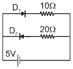
- 10.75 A
- 2zero
- 30.25 A
- 40.5 A
Show answer and solution
Correct: option 4, 0.5 A
is forward biased and, being ideal, acts as a plain wire, so the branch conducts. is reverse biased and blocks the branch. The battery current is therefore .
Question 66AIPMT 2012 Prelims, Q7
In a CE transistor amplifier, the audio signal voltage across the collector resistance of is 2 V. If the base resistance is and the current amplification of the transistor is 100, the input signal voltage is:
- 10.1 V
- 21.0 V
- 31 mV
- 410 mV
Show answer and solution
Correct: option 4, 10 mV
The collector current is . With a current gain of 100 the base current is . The input voltage is .
Question 67AIPMT 2012 Prelims, Q21
C and Si both have same lattice structure, having 4 bonding electrons in each. However, C is insulator whereas Si is intrinsic semiconductor. This is because:
- 1In case of C the valence band is not completely filled at absolute zero temperature.
- 2In case of C the conduction band is partly filled even at absolute zero temperature.
- 3The four bonding electrons in the case of C lie in the second orbit, whereas in the case of Si they lie in the third.
- 4The four bonding electrons in the case of C lie in the third orbit, whereas for Si they lie in the fourth orbit.
Show answer and solution
Correct: option 3, The four bonding electrons in the case of C lie in the second orbit, whereas in the case of Si they lie in the third.
Carbon is and silicon is , so the four bonding electrons are in the second orbit in C and in the third orbit in Si. The electrons of C are closer to the nucleus and more tightly bound, which gives a much larger energy gap (about 5.4 eV against 1.1 eV for Si), so C is an insulator.
Question 68AIPMT 2012 Prelims, Q38
Transfer characteristics [output voltage () vs input voltage ()] for a base biased transistor in CE configuration is as shown in the figure. For using transistor as a switch, it is used:
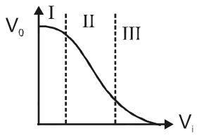
- 1in region III
- 2both in region (I) and (III)
- 3in region II
- 4in region I
Show answer and solution
Correct: option 2, both in region (I) and (III)
Region I is cut-off (low input, no collector current, high output) and region III is saturation (high input, large collector current, low output). A switch works by being driven between these two states, off in cut-off and on in saturation. Region II is the active region, used for amplification.
Question 69AIPMT 2012 Prelims, Q43
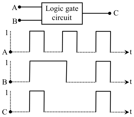
The figure shows a logic circuit with two inputs A and B and the output C. The voltage wave forms across A, B and C are as given. The logic circuit gate is:
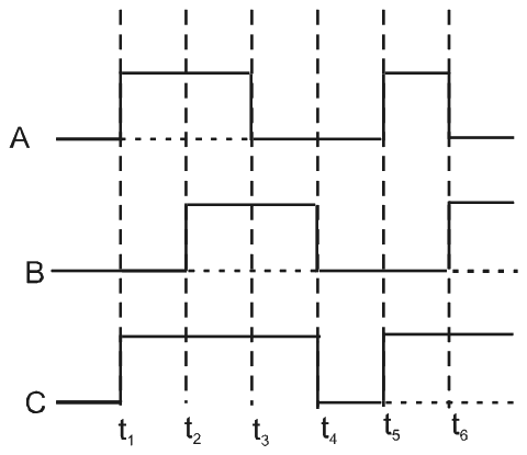
- 1OR gate
- 2NOR gate
- 3AND gate
- 4NAND gate
Show answer and solution
Correct: option 1, OR gate
Read the levels interval by interval. From to only A is high and C is high; from to both are high and C is high; from to only B is high and C is high; from to both are low and C is low. The output is high whenever at least one input is high, which is an OR gate.
Question 70AIPMT 2012 Mains, Q29
The input resistance of a silicon transistor is . Base current is changed by which results in a change in collector current by 2 mA. This transistor is used as a common emitter amplifier with a load resistance of . The voltage gain of the amplifier is:
- 12000
- 23000
- 34000
- 41000
Show answer and solution
Correct: option 1, 2000
Current gain . Voltage gain of a common emitter amplifier is .
Question 71AIPMT 2012 Mains, Q30
To get an output Y = 1 in given circuit which of the following input will be correct:
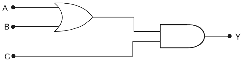
- 1A = 1, B = 0, C = 0
- 2A = 1, B = 0, C = 1
- 3A = 1, B = 1, C = 0
- 4A = 0, B = 1, C = 0
Show answer and solution
Correct: option 2, A = 1, B = 0, C = 1
A and B feed an OR gate, and its output goes with C into an AND gate, so . Y is 1 only when C = 1 and at least one of A and B is 1. Among the options only A = 1, B = 0, C = 1 has C = 1.
Question 72AIPMT 2011 Prelims, Q176
A transistor is operated in common emitter configuration at V such that a change in the base current from 100 A to 300 A produces a change in the collector current from 10 mA to 20 mA. The current gain is:
- 150
- 275
- 3100
- 425
Show answer and solution
Correct: option 1, 50
Current gain .
Question 73AIPMT 2011 Prelims, Q177
In forward biasing of the p-n junction:
- 1the positive terminal of the battery is connected to p-side and the depletion region becomes thick
- 2the positive terminal of the battery is connected to n-side and the depletion region becomes thin
- 3the positive terminal of the battery is connected to n-side and the depletion region becomes thick
- 4the positive terminal of the battery is connected to p-side and the depletion region becomes thin
Show answer and solution
Correct: option 4, the positive terminal of the battery is connected to p-side and the depletion region becomes thin
In forward bias the positive terminal goes to the p-side and the negative terminal to the n-side. The applied voltage opposes the barrier potential, pushing holes and electrons towards the junction, so the depletion region becomes thinner.
Question 74AIPMT 2011 Prelims, Q180
Symbolic representation of four logic gate are shown as:

Pick out which ones are for AND, NAND and NOT gates, respectively:
- 1(ii), (iii) and (iv)
- 2(iii), (ii) and (i)
- 3(iii), (iii) and (iv)
- 4(ii), (iv) and (iii)
Show answer and solution
Correct: option 4, (ii), (iv) and (iii)
(i) has the curved back and pointed front of an OR gate. (ii) is the D-shaped AND gate. (iii) is a triangle with a small circle at its output, the NOT gate. (iv) is an AND shape with a circle at the output, the NAND gate. So AND, NAND and NOT are (ii), (iv) and (iii).
Question 75AIPMT 2011 Prelims, Q200
If a small amount of antimony is added to germanium crystal:
- 1It becomes a p-type semiconductor
- 2the antimony becomes an acceptor atom
- 3there will be more free electrons than holes in the semiconductor
- 4its resistance is increased
Show answer and solution
Correct: option 3, there will be more free electrons than holes in the semiconductor
Antimony has five valence electrons. In germanium four of them form bonds and the fifth is free, so antimony is a donor and the crystal becomes n-type, with more free electrons than holes. Its resistance falls, not rises.
Question 76AIPMT 2011 Mains, Q92
In the following figure, the diodes which are forward biased, are:
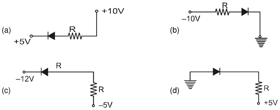
- 1(c) only
- 2(c) and (a)
- 3(b) and (d)
- 4(a), (b) and (d)
Show answer and solution
Correct: option 2, (c) and (a)
A diode is forward biased when its p-side (the base of the triangle in the symbol) is at a higher potential than its n-side (the bar). In (a) the p-side is towards +10 V and the n-side at +5 V, and in (c) the p-side is towards -5 V and the n-side at -12 V, so both are forward biased. In (b) the p-side is at -10 V with the n-side earthed, and in (d) the p-side is earthed with the n-side towards +5 V, so both are reverse biased.
Question 77AIPMT 2011 Mains, Q100
Pure Si at 500K has equal number of electron () and hole () concentrations of . Doping by indium increases to . The doped semiconductor is of:
- 1n-type with electron concentration
- 2p-type with electron concentration
- 3n-type with electron concentration
- 4p-type having electron concentrations
Show answer and solution
Correct: option 4, p-type having electron concentrations
Indium is trivalent, so it adds holes and the semiconductor becomes p-type. The product of the carrier concentrations stays equal to : .
Question 78AIPMT 2011 Mains, Q102
A zener diode, having breakdown voltage equal to 15V, is used in a voltage regulator circuit shown in figure. The current through the diode is:
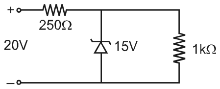
- 110 mA
- 215 mA
- 320 mA
- 45 mA
Show answer and solution
Correct: option 4, 5 mA
The zener holds 15 V across itself and the 1 kΩ load, so the load current is mA. The remaining V falls across the 250 Ω series resistor, so the supply current is mA. The zener carries the difference, mA.
Question 79AIPMT 2010 Mains, Q2
The following figure shows a logic gate circuit with two inputs A and B and the output Y. The voltage wave forms of A, B and Y are as given.
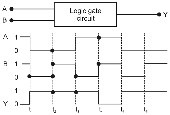
- 1NOR gate
- 2OR gate
- 3AND gate
- 4NAND gate
Show answer and solution
Correct: option 4, NAND gate
Read the three wave forms interval by interval. Y is 0 only in the intervals where A and B are both 1 (before and between and ); whenever at least one input is 0 the output is 1. An output that is low only when both inputs are high is that of a NAND gate.
Question 80AIPMT 2010 Mains, Q10
For transistor action
(1) Base, emitter and collector regions should have similar size and doping concentrations.
(2) The base region must be very thin and lightly doped.
(3) The emitter-base junction is forward biased and base-collector junction is reverse biased
(4) Both the emitter-base junction as well as the base-collector junction are forward biased
- 1(4) and (1)
- 2(1) and (2)
- 3(2) and (3)
- 4(3) and (4)
Show answer and solution
Correct: option 3, (2) and (3)
In a transistor the emitter is heavily doped, the base is very thin and lightly doped, and the collector is the largest region with moderate doping, so statement (1) is wrong and (2) is right. In the active state the emitter-base junction is forward biased and the base-collector junction is reverse biased, so (3) is right and (4) is wrong. The correct pair is (2) and (3).
Question 81AIPMT 2010 Prelims, Q4
Which one of the following statement is false?
- 1Pure Si doped with trivalent impurities gives a p-type semiconductor.
- 2Majority carriers in a n-type semiconductor are holes.
- 3Minority carriers in a p-type semiconductor are electrons.
- 4The resistance of intrinsic semiconductor decreases with increase of temperature.
Show answer and solution
Correct: option 2, Majority carriers in a n-type semiconductor are holes.
An n-type semiconductor is made with pentavalent (donor) impurities, so its majority carriers are electrons and holes are the minority carriers. Statement (2) is therefore false. The other three are true: trivalent doping gives p-type material, electrons are the minority carriers there, and heating an intrinsic semiconductor frees more carriers and lowers its resistance.
Question 82AIPMT 2010 Prelims, Q17
Which one of the following bonds produces a solid that reflects light in the visible region and whose electrical conductivity decreases with temperature and has high melting point?
- 1metallic bonding
- 2van der Waals' bonding
- 3ionic bonding
- 4covalent bonding
Show answer and solution
Correct: option 1, metallic bonding
These are the properties of a metal. Its free electrons reflect visible light and give it lustre, its conductivity falls as the temperature rises because the electrons are scattered more by the vibrating lattice, and metallic bonding is strong enough to give a high melting point. Ionic, covalent and van der Waals' solids are not shiny conductors of this kind.
Question 83AIPMT 2010 Prelims, Q23
The device that act as a complete electronic circuit is
- 1junction diode
- 2integrated circuit
- 3junction transistor
- 4zener diode
Show answer and solution
Correct: option 2, integrated circuit
An integrated circuit has many components (transistors, diodes, resistors, capacitors) and their connections built on a single chip, so it works as a complete circuit by itself. A diode, a zener diode or a transistor is only a single component of a circuit.
Question 84AIPMT 2010 Prelims, Q41
A common emitter amplifier has a voltage gain of 50, an input impedance of 100 and an output impedance of 200 . The power gain of the amplifier is
- 1500
- 21000
- 31250
- 450
Show answer and solution
Correct: option 3, 1250
Voltage gain = current gain × resistance gain, and the resistance gain is , so the current gain is . Power gain = voltage gain × current gain .
Question 85AIPMT 2010 Prelims, Q50
To get an output Y = 1 from the circuit shown below the input must be
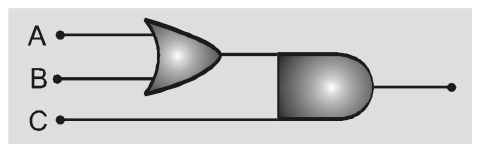
- 1A = 0, B = 1, C = 0
- 2A = 0, B = 0, C = 1
- 3A = 1, B = 0, C = 1
- 4A = 1, B = 0, C = 0
Show answer and solution
Correct: option 3, A = 1, B = 0, C = 1
A and B go into an OR gate, and its output goes with C into an AND gate, so . Y is 1 only when C = 1 and at least one of A and B is 1. Of the options only A = 1, B = 0, C = 1 satisfies this.
Question 86AIPMT 2009 Prelims, Q8
The symbolic representation of four logic gates are given below:
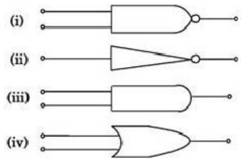
The logic symbols for OR, NOT and NAND gates are respectively:
- 1(iv), (i), (iii)
- 2(iv), (ii), (i)
- 3(i), (iii), (iv)
- 4(iii), (iv), (ii)
Show answer and solution
Correct: option 2, (iv), (ii), (i)
Symbol (i) is an AND shape with a bubble at the output, which is NAND. Symbol (ii) is a triangle with a bubble, which is NOT. Symbol (iii) is the plain AND gate and symbol (iv), with the curved input side, is OR. So OR, NOT and NAND are (iv), (ii) and (i).
Question 87AIPMT 2009 Prelims, Q11
A p-n photodiode is fabricated from a semiconductor with a band gap of 2.5 eV. It can detect a signal of wavelength:
- 14000 nm
- 26000 nm
- 34000 Å
- 46000 Å
Show answer and solution
Correct: option 3, 4000 Å
The photon energy must be at least the band gap, so the wavelength must not exceed Å. Of the options only 4000 Å is shorter than this, so only that signal is detected.
Question 88AIPMT 2009 Prelims, Q13
A transistor is operated in common-emitter configuration at V such that a change in the base current from 100 µA to 200 µA produces a change in the collector current from 5 mA to 10 mA. The current gain is:
- 1100
- 2150
- 350
- 475
Show answer and solution
Correct: option 3, 50
The common-emitter current gain is .
Question 89AIPMT 2009 Prelims, Q36
Sodium has body centred packing. Distance between two nearest atoms is 3.7 Å. The lattice parameter is:
- 14.3 Å
- 23.0 Å
- 38.6 Å
- 46.8 Å
Show answer and solution
Correct: option 1, 4.3 Å
In a body centred cubic cell the nearest neighbours are a corner atom and the body-centre atom, half a body diagonal apart: . So Å.
Question 90AIPMT 2008 Prelims, Q47
The voltage gain of an amplifier with 9% negative feedback is 10. The voltage gain without feedback will be
- 1100
- 290
- 310
- 41.25
Show answer and solution
Correct: option 1, 100
With negative feedback the gain is , where is the fraction of the output fed back. gives , so .
Question 91AIPMT 2008 Prelims, Q48
If the lattice parameter for a crystalline structure is 3.6 Å, then the atomic radius in fcc crystal is
- 11.27 Å
- 21.81 Å
- 32.10 Å
- 42.92 Å
Show answer and solution
Correct: option 1, 1.27 Å
In a face-centred cubic cell the atoms touch along a face diagonal, which holds four radii: . So Å.
Question 92AIPMT 2008 Prelims, Q49
- 1OR gate
- 2AND gate
- 3NAND gate
- 4NOR gate
Show answer and solution
Correct: option 4, NOR gate
The NAND gate has its two inputs joined, so it acts as a NOT gate. The NOR output therefore passes through two inversions in a row (the NAND used as NOT, then the NOT gate), which cancel. The output is the same as that of the first gate, so the circuit is a NOR gate.
Question 93AIPMT 2008 Prelims, Q50
A p-n photodiode is made of a material with a band gap of 2.0 eV. The minimum frequency of the radiation that can be absorbed by the material is nearly
- 1 Hz
- 2 Hz
- 3 Hz
- 4 Hz
Show answer and solution
Correct: option 3, Hz
A photon is absorbed only if its energy is at least the band gap: . So Hz, nearly Hz.
Question 94AIPMT 2007 Prelims, Q197
In the energy band diagram of a material shown below, the open circles and filled circles denote holes and electrons respectively. The material is
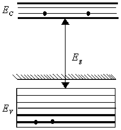
- 1an n-type semiconductor
- 2a p-type semiconductor
- 3an insulator
- 4a metal
Show answer and solution
Correct: option 2, a p-type semiconductor
The diagram has an extra energy level lying just above the valence band, far below the conduction band. Such a level is an acceptor level: it takes electrons from the valence band and leaves holes there as the majority carriers. That is a p-type semiconductor, option (2).
Question 95AIPMT 2007 Prelims, Q198
A common emitter amplifier has a voltage gain of 50, an input impedance of 100 Ω and an output impedance of 200 Ω. The power gain of the amplifier is
- 1100
- 2500
- 31000
- 41250
Show answer and solution
Correct: option 4, 1250
Voltage gain , so the current gain is . Power gain is current gain times voltage gain: , option (4).
Question 96AIPMT 2007 Prelims, Q200
For a cubic crystal structure which one of the following relations indicating the cell characteristics is correct?
- 1 and
- 2 and
- 3 and
- 4 and
Show answer and solution
Correct: option 1, and
A cubic unit cell is a cube: its three edges are equal and all three angles between them are right angles, so and . This is option (1).
Question 97AIPMT 2006 Prelims, Q20
A transistor is operated in common emitter configuration at constant collector voltage such that a change in the base current from 100 µA to 150 µA produces a change in the collector current from 5 mA to 10 mA. The current gain () is:-
- 167
- 275
- 3100
- 450
Show answer and solution
Correct: option 3, 100
The a.c. current gain is .
Question 98AIPMT 2006 Prelims, Q21
A forward biased diode is:-
- 1

- 2

- 3

- 4

Show answer and solution
Correct: option 4
A diode is forward biased when its p-side (the base of the arrow in the symbol) is at a higher potential than its n-side. In every option the arrow points to the right, so the left end must be the higher one. That is true only for on the left and on the right; in the other three the left end is lower, so those diodes are reverse biased.
Question 99AIPMT 2006 Prelims, Q27
The following figure shows a logic gate circuit with two inputs A and B and the output C. The voltage waveforms of A, B and C are as shown below-
The logic circuit gate is:
- 1AND gate
- 2NAND gate
- 3NOR gate
- 4OR gate
Show answer and solution
Correct: option 1, AND gate
Compare the waveforms pulse by pulse. During the first and third pulses of A, B is also high and C is high. During the second pulse of A, B is low and C is low; when both inputs are low C is low. The output is high only when both inputs are high, which is the AND gate.
Question 100AIPMT 2005 Prelims, Q2
- 1Rectification
- 2Stabilisation
- 3Amplification
- 4Producing oscillations in an oscillator
Show answer and solution
Correct: option 2, Stabilisation
In reverse breakdown the voltage across a Zener diode stays almost constant while the current through it changes over a wide range. This makes it a voltage regulator, so it is used for stabilisation.
Question 101AIPMT 2005 Prelims, Q29
Copper has face centered cubic (fcc) lattice with interatomic spacing equal to 2.54Å. The value of lattice constant for this lattice is
- 13.59Å
- 22.54 Å
- 31.27 Å
- 45.08 Å
Show answer and solution
Correct: option 1, 3.59Å
In an fcc lattice nearest neighbours touch along the face diagonal, so the interatomic spacing is . Hence Å.
Question 102AIPMT 2005 Prelims, Q35
Choose the only false statement from the following
- 1The resistivity of a semiconductor increases with increase in temperature
- 2Substances with energy gap of the order of 10eV are insulators.
- 3In conductors the valence and conduction bands may overlap
- 4The conductivity of a semiconductor increases with increase in temperature.
Show answer and solution
Correct: option 1, The resistivity of a semiconductor increases with increase in temperature
Heating a semiconductor frees more electrons and holes, so its conductivity rises and its resistivity falls. The statement that resistivity increases with temperature is therefore false. The other three are true: a gap near 10 eV means an insulator, and bands can overlap in conductors.
Question 103AIPMT 2005 Prelims, Q38
Carbon, Silicon and Germanium atoms have four valence electrons each. Their valence and conduction bands are separated by energy band gaps represented by , and respectively. Which one of the following relationships is true in their case
- 1
- 2
- 3
- 4
Show answer and solution
Correct: option 2,
The band gap falls down the group: carbon (diamond) about 5.5 eV, silicon about 1.1 eV, germanium about 0.7 eV. Carbon is an insulator while Si and Ge are semiconductors, so the gap of carbon is greater than that of silicon.
Question 104AIPMT 2005 Prelims, Q45
Application of a forward bias to a p-n junction
- 1Widens the depletion zone
- 2Increases the number of donors on the n side
- 3Increases the potential difference across the depletion zone
- 4Increases the electric field in the depletion zone
Show answer and solution
Correct: option 2, Increases the number of donors on the n side
Forward bias opposes the built-in barrier: the depletion zone becomes narrower, and the potential difference and electric field across it fall, so options (1), (3) and (4) are wrong. The key takes the remaining option (2), read as the forward bias pushing more majority carriers on the n side towards the junction. Strictly the number of donor atoms is fixed by doping and does not change, so the keyed option is the accepted answer by elimination.
Question 105AIPMT 2004 Prelims, Q8
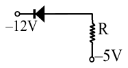
Of the diodes shown in the following diagrams, which one of the diode is reverse biased?
- 1
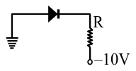
- 2
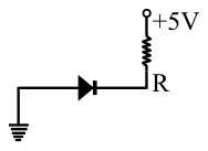
- 3
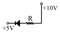
- 4
Show answer and solution
Correct: option 2
A diode is reverse biased when its p-side (the base of the arrow) is at a lower potential than its n-side (the bar). In (2) the p-side is earthed (0 V) and the n-side is connected through R to +5 V, so it is reverse biased. In (1) the p-side is at 0 V and the n-side goes to V; in (3) the p-side goes to +10 V and the n-side is at +5 V; in (4) the p-side goes to V and the n-side is at V. Those three are forward biased.
Question 106AIPMT 2004 Prelims, Q15
In semiconductors at a room temperature
- 1The valence band is completely filled and the conduction band is partially filled
- 2The valence band is completely filled
- 3The conduction band is completely empty
- 4The valence band is partially empty and the conduction band is partially filled
Show answer and solution
Correct: option 4, The valence band is partially empty and the conduction band is partially filled
The energy gap of a semiconductor is small (about 1 eV), so at room temperature some electrons are thermally excited from the valence band to the conduction band. This leaves holes in the valence band (partially empty) and electrons in the conduction band (partially filled).
Question 107AIPMT 2004 Prelims, Q16
The peak voltage in the output of a half wave diode rectifier fed with a sinusoidal signal without filter is 10V. The d.c. component of the output voltage is:-
- 1 V
- 210 V
- 3 V
- 4 V
Show answer and solution
Correct: option 1, V
The output of a half wave rectifier is a half sine pulse in one half cycle and zero in the other. Its average over a full cycle is V.
Question 108AIPMT 2004 Prelims, Q41
In a p–n junction photo cell, the value of the photo electromotive force produced by monochromatic light is proportional to:-
- 1The intensity of the light falling on the cell
- 2The frequency of the light falling on the cell
- 3The voltage applied at the p–n junction
- 4The barrier voltage at the p–n junction
Show answer and solution
Correct: option 1, The intensity of the light falling on the cell
Each absorbed photon creates an electron-hole pair, so the number of charge carriers generated per second, and with it the photo-emf, depends on the number of photons arriving per second, that is on the intensity of the light. For a given monochromatic light the frequency is fixed and no external voltage is applied.
Question 109AIPMT 2004 Prelims, Q43
The output of OR gate is 1:-
- 1If either or both inputs are 1
- 2Only if both inputs are 1
- 3If either input is zero
- 4If both inputs are zero
Show answer and solution
Correct: option 1, If either or both inputs are 1
For an OR gate : the output is 0 only when both inputs are 0, and is 1 when either input or both inputs are 1.
Question 110AIPMT 2003 Prelims, Q39
Reverse bias applied to a junction diode
- 1Lowers the potential barrier
- 2raises the potential barrier
- 3increases the majority carrier current
- 4increases the minority carrier current
Show answer and solution
Correct: option 2, raises the potential barrier
In reverse bias the applied voltage acts in the same direction as the barrier potential, so the barrier becomes higher and the depletion layer wider. Majority carriers are then blocked, and the small minority-carrier current stays almost the same.
Question 111AIPMT 2003 Prelims, Q42
A n-p-n transistor conducts when
- 1both collector and emitter are positive with respect to the base
- 2collector is positive and emitter is negative with respect to the base
- 3collector is positive and emitter is at same potential as the base
- 4both collector and emitter are negative with respect to the base
Show answer and solution
Correct: option 2, collector is positive and emitter is negative with respect to the base
A transistor conducts with the emitter-base junction forward biased and the collector-base junction reverse biased. In an n-p-n transistor the base is p-type, so the n-type emitter must be negative and the n-type collector positive with respect to the base.
Question 112AIPMT 2003 Prelims, Q45
If a full wave rectifier circuit is operating from 50 Hz mains, the fundamental frequency in the ripple will be:
- 125 Hz
- 250 Hz
- 370.7 Hz
- 4100 Hz
Show answer and solution
Correct: option 4, 100 Hz
A full wave rectifier turns both half-cycles into pulses of the same sign, so the output repeats twice in each input cycle. The ripple frequency is Hz.
Question 113AIPMT 2003 Prelims, Q46
Barrier potential of a p-n junction diode does not depend on -
- 1diode design
- 2temperature
- 3forward bias
- 4doping density
Show answer and solution
Correct: option 1, diode design
The barrier potential is fixed by the material, the doping density on the two sides and the temperature, and the height of the barrier is lowered by a forward bias. It does not depend on the shape or design of the diode.
Question 114AIPMT 2003 Prelims, Q50
Following diagram performs the logic function of:

- 1AND gate
- 2NAND gate
- 3OR gate
- 4XOR gate
Show answer and solution
Correct: option 1, AND gate
The first gate is a NAND gate, giving . The second NAND gate has this single signal as its input, so it works as a NOT gate and inverts it: , the AND function.
Question 115AIPMT 2002 Prelims, Q31
For a transistor = 0.96, then current gain for common emitter configuration:-
- 112
- 26
- 348
- 424
Show answer and solution
Correct: option 4, 24
. The common emitter current gain is .
Question 116AIPMT 2002 Prelims, Q34
- 1High potential at N side and low potential at P side
- 2High potential at P side and low potential at N side
- 3P and N both are at same potential
- 4Undetermined
Show answer and solution
Correct: option 1, High potential at N side and low potential at P side
At an unbiased junction, electrons diffuse from N to P and holes from P to N. This leaves fixed positive donor ions on the N side and fixed negative acceptor ions on the P side of the depletion layer. So the N side is at the higher potential and the P side at the lower potential.
Question 117AIPMT 2002 Prelims, Q35
The given truth table is for which logic gate:-
- 1NAND
- 2XOR
- 3NOR
- 4OR
Show answer and solution
Correct: option 1, NAND
The output is 0 only when both inputs are 1 and is 1 in every other case. That is the complement of AND, , which is the NAND gate.
Question 118AIPMT 2002 Prelims, Q36
For the given circuit of P-N junction diode which is correct:-
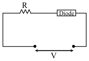
- 1In F.B. the voltage across R is V
- 2In R.B. the voltage across R is V
- 3In F.B. the voltage across R is 2 V
- 4In R.B. the voltage across R is 2 V
Show answer and solution
Correct: option 1, In F.B. the voltage across R is V
In forward bias an ideal diode conducts with negligible resistance and negligible voltage drop, so the whole applied voltage V appears across R. In reverse bias the diode does not conduct, no current flows and the voltage across R is zero.
Question 119AIPMT 2001 Prelims, Q2
Following truth table represent which logic gate –
- 1XOR
- 2NOT
- 3NAND
- 4AND
Show answer and solution
Correct: option 3, NAND
The output is 0 only when both inputs are 1 and is 1 in every other case. That is the AND output inverted, , which is a NAND gate.
Question 120AIPMT 2001 Prelims, Q10
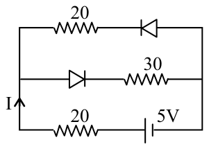
The current (I) in the circuit will be:
- 1 A
- 2 A
- 3 A
- 4 A
Show answer and solution
Correct: option 2, A
For the direction of the current I, the diode in the 30 branch is forward biased and the diode in the upper 20 branch is reverse biased, so the upper branch carries no current. Treating the diodes as ideal, the current flows through 30 and the lower 20 in series: A.
Question 121AIPMT 2001 Prelims, Q36
For a common emitter circuit if then current gain for common emitter circuit will be:
- 149
- 298
- 34.9
- 425.5
Show answer and solution
Correct: option 1, 49
Here . The common emitter current gain is .
Question 122AIPMT 2000 Prelims, Q31
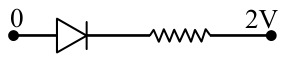
From the following diode circuit. Which diode in forward biased condition:
- 1

- 2
- 3
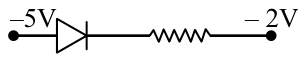
- 4
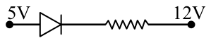
Show answer and solution
Correct: option 1
A diode is forward biased when its p-side (the base of the triangle, on the left in each picture) is at a higher potential than its n-side. In (1) the left end is at 0 V and the right end at −2 V, so the p-side is higher: forward biased. In (2) 0 V against 2 V, in (3) −5 V against −2 V and in (4) 5 V against 12 V the left end is lower, so those are reverse biased.
Question 123AIPMT 2000 Prelims, Q32
Given Truth table is correct for:
- 1NAND
- 2AND
- 3NOR
- 4OR
Show answer and solution
Correct: option 2, AND
The output is 1 only when both inputs are 1 and is 0 in every other row. That is , the AND gate.
Question 124AIPMT 2000 Prelims, Q45
The correct relation for , for a transistor:
- 1
- 2
- 3
- 4
Show answer and solution
Correct: option 2,
, and . So .
Question 125AIPMT 1999 Prelims, Q18
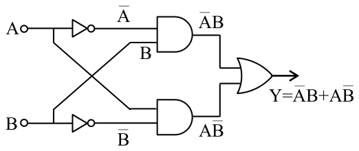
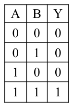
The truth table for the following network is:
- 1
- 2
- 3
- 4None of the above
Show answer and solution
Correct: option 2
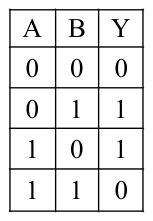
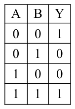
The upper AND gate gives and the lower AND gate gives ; the OR gate adds them, so . This is the exclusive-OR function: only when the two inputs are different. So the outputs for (A, B) = (0,0), (0,1), (1,0), (1,1) are 0, 1, 1, 0, which is the table in option (2).
Question 126AIPMT 1999 Prelims, Q19
- 1Half wave rectifier
- 2Full wave rectifier
- 3A.C. voltage stabilizer
- 4D.C. voltage stabilizer
Show answer and solution
Correct: option 4, D.C. voltage stabilizer
In reverse breakdown the voltage across a Zener diode stays almost constant while the current through it changes over a wide range. Connected in reverse bias across a load, it therefore holds the d.c. output voltage steady, so it is used as a D.C. voltage stabilizer (regulator).
Question 127AIPMT 1999 Prelims, Q20
Depletion layer has (for an unbiased PN junction) -
- 1Electrons
- 2Holes
- 3Static ions
- 4Neutral atoms
Show answer and solution
Correct: option 3, Static ions
Near the junction, electrons from the n-side and holes from the p-side diffuse across and recombine. This leaves the region without mobile charge carriers; what remains are the fixed (immobile) donor and acceptor ions. So the depletion layer contains static ions.
Question 128AIPMT 1998 Prelims, Q3
Following table is for which logic gate:
| Input A | Input B | Output C |
|---|
| 0 | 0 | 1 |
| 0 | 1 | 1 |
| 1 | 0 | 1 |
| 1 | 1 | 0 |
- 1AND
- 2OR
- 3NAND
- 4NOT
Show answer and solution
Correct: option 3, NAND
The output is 0 only when both inputs are 1 and is 1 in every other case. That is the AND output inverted, , which is the NAND gate.
Question 129AIPMT 1998 Prelims, Q4
- 1AND
- 2NAND
- 3EX-OR
- 4OR
Show answer and solution
Correct: option 2, NAND
The symbol is the D-shaped AND gate with a small circle (an inverter bubble) at its output. An AND gate followed by NOT gives , the NAND gate.
Question 130AIPMT 1998 Prelims, Q18
One part of a device is connected with the negative terminal of a battery and another part is connected with the positive terminal of a battery. If their ends now altered, current does not flow in circuit, then the device will be:
- 1P–N Junction
- 2Transistor
- 3Zener diode
- 4Triode
Show answer and solution
Correct: option 1, P–N Junction
A device that conducts for one polarity of the battery and blocks when the connections are reversed is a rectifier. A P–N junction does exactly this: it conducts in forward bias and passes practically no current in reverse bias.
Question 131AIPMT 1998 Prelims, Q46
The cause of potential barrier in a P–N junction diode is:
- 1Concentration of positive and negative ions near the junction
- 2Concentration of positive charges near the junction
- 3Depletion of negative charges near the junction
- 4Increment in concentration of holes and electrons near the junction
Show answer and solution
Correct: option 1, Concentration of positive and negative ions near the junction
Near the junction, electrons and holes diffuse across and recombine. This leaves fixed positive donor ions on the N side and fixed negative acceptor ions on the P side. These two layers of uncovered ions set up the electric field, and so the potential barrier, across the junction.
Question 132AIPMT 1998 Prelims, Q47
Common emitter circuit is used as amplifier, its current gain is 50. If input resistance is and input voltage is 5 volt then output current will be:
- 1250 mA
- 230 mA
- 350 mA
- 4100 mA
Show answer and solution
Correct: option 1, 250 mA
The input (base) current is mA. The output (collector) current is the current gain times this: mA.